
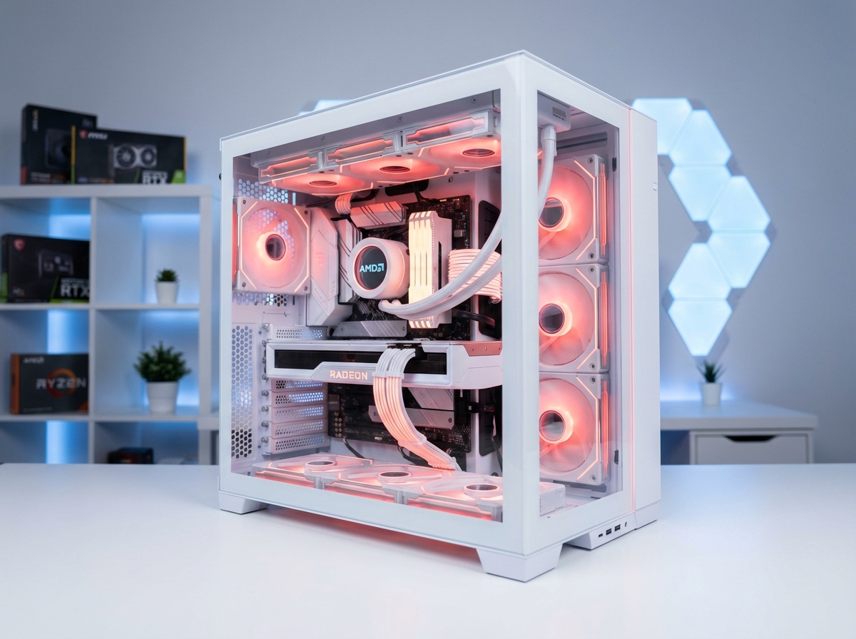

AMD's Zen 7 architecture is shaping up to be the most consequential redesign the company has undertaken since the original chiplet-based Zen 2 launched in 2019. While Zen 6 has yet to reach consumer hands — expected in late 2026 — a substantial volume of detailed, credible leaks sourced primarily from Moore's Law Is Dead (MLID) has painted a remarkably complete picture of what Zen 7 will deliver across desktop, mobile, and server markets.
The scope of architectural changes reported is significant: a move to TSMC's A14 1.4nm process node, a doubling of cores per chiplet from 8 to 16, a doubling of L2 cache per core, expanded L3 V-Cache with 224MB configurations, new ISA extensions for AI acceleration, and an entirely new die-stacking chiplet architecture for the server segment that enables 288-core EPYC processors.
This article compiles and analyzes every confirmed and leaked detail about AMD Zen 7, organized by product family and architectural layer, providing the most thorough technical breakdown available outside of AMD's internal documentation.
Disclosure
All Zen 7 specifications discussed below originate from industry leaks and should be treated as pre-release information subject to change. AMD has not officially confirmed Zen 7 architectural details beyond its high-level CPU roadmap.
AMD Zen 7 Release Timeline: When to Expect Grimlock CPUs
The Zen 7-based EPYC processors are slated to launch in the first half of 2028, with the Ryzen desktop and mobility chips likely landing in the latter half of the same year. This timeline is directly tied to TSMC's A14 manufacturing schedule. The primary manufacturing process for Zen 7 is TSMC's A14 process — not the 1.6nm A16 process, which is actually a variant of the 2nm process enhanced with backside power delivery technology. The 1.4nm A14 process is a completely new generation, but without backside power delivery.
The intermediate Zen 6 architecture will use TSMC's N2P (2nm) node, with desktop launches expected in late 2026 following earlier APU and EPYC rollouts. Zen 7 on A14 follows approximately 18–24 months later, maintaining AMD's historical cadence of one major architecture per two years. The IOD used for Zen 7 chips is reportedly the same hardware that will be utilized for Zen 6 processors in 2027, suggesting a long-term platform commitment.
Zen 7 Launch Timeline Estimate
| Product Segment | Codename | Expected Launch |
|---|---|---|
| EPYC Server (Florence) | Steamboat | H1 2028 |
| Ryzen Desktop (Grimlock Ridge) | Silverton / Silverking | H2 2028 |
| Ryzen Mobile (Grimlock Point / Halo) | Grimlock Halo, Grimlock Point | H2 2028 |
TSMC A14 Node: What 1.4nm Means for Zen 7 Performance and Density
The Zen 7 "Grimlock" family is expected to be fabbed on TSMC's next-generation A14 node. This is a 1.4nm-class process node (the "A" stands for Angstrom). Moving to 1.4nm represents a massive leap in transistor density, which explains how AMD plans to pack 32 cores onto dies that are physically smaller than today's chips.
TSMC's A14 node represents a genuine generational transition rather than an incremental refinement. The naming convention reflects TSMC's shift to Angstrom-scale nomenclature (1 Angstrom = 0.1 nanometers), similar to the move Intel has made with its process node branding. Critically, A14 does not incorporate backside power delivery — a technology that routes power supply rails to the underside of the silicon die, freeing front-side routing resources for signal interconnects and improving power delivery efficiency. AMD apparently doesn't want to deploy this technology for its mainstream-market processors yet.
Despite the absence of backside power delivery, A14's transistor density improvements over N2/N2P are substantial. The leaks suggest that AMD's 16-core Silverton CCD measures approximately 98mm² on A14. For comparison, AMD's current 8-core Zen 5 CCD (on TSMC N4P) measures approximately 70–71mm². Doubling the core count while adding 50% die area reflects exceptional density scaling from N4P to A14.
Based on document fragments shown by MLID, the CPU chiplet with 16 cores could have 19 metal layers and use HP (High Performance) libraries. The HP library designation indicates AMD is prioritizing clock speed and IPC rather than optimizing for power efficiency — consistent with the reported 7 GHz clock speed target for Silverton-based gaming SKUs.
Zen 7 IPC Gains: 15–25% Uplift Over Zen 6, With 8% From Cache Alone
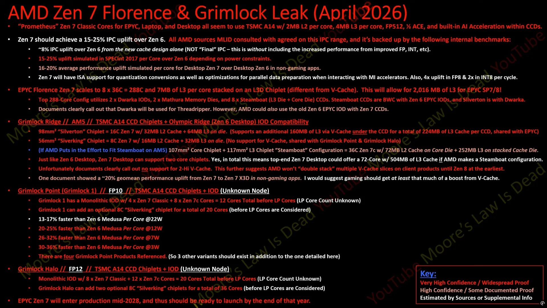
The headline performance claim for Zen 7 is its IPC (Instructions Per Cycle) improvement. The IPC gain over Zen 6 is estimated to land somewhere between 15–25%. It's worth noting that just by reorganizing the cache subsystem, AMD managed to get an 8% speed bump without even touching the compute cores themselves.
Breaking down the sources of the projected IPC gains:
- Cache hierarchy redesign: 8% IPC uplift attributable solely to cache changes (doubled L2 per core, larger unified L3)
- Core microarchitecture improvements: The remaining 7–17% IPC delta from execution unit redesign, branch prediction improvements, prefetcher enhancements, and memory subsystem latency reductions
- New ISA extensions: AI-targeted instructions and expanded matrix operation support contribute to specialized workload acceleration beyond general IPC metrics
Zen 7 desktop will offer up to a 20% improvement in single-threaded performance and 67% in multi-core over Zen 6. In SPEC2017 synthetic benchmarks for desktop versions, simulations show a 16–20% uplift in non-gaming workloads.
The 67% multi-core improvement figure is not purely architectural — it reflects the combination of IPC gains plus the doubling of cores per CCD (from 8 in Zen 5 to 16 in Zen 7), which doubles multi-threaded throughput in core-scaling workloads before any per-core performance improvement is applied.
Mobile Efficiency Gains: Dramatic Performance-Per-Watt Improvements
On the laptop side, Grimlock Point and Grimlock Halo could bring forth notable increases in performance-per-watt:
- +36% performance-per-watt at 3 W
- +32% at 7 W
- +25% at 12 W
- +17% at 22 W
The inverse relationship between wattage and efficiency gain is characteristic of process node improvements: at ultra-low power levels where current nodes are heavily voltage-limited, A14's superior voltage-frequency curve provides disproportionate efficiency benefits. This is what makes A14 particularly compelling for mobile products, where the 3W–12W range represents always-on background processing tasks.
Complete AMD Zen 7 Architecture Diagram
flowchart TD
    A14["TSMC A14 Node
1.4nm Class
HVM: 2028"]

    subgraph Desktop["Desktop — Grimlock Ridge AM5"]
        Silverton["Silverton CCD
16 Zen 7 Cores
32MB L2 / 64MB L3
+ 160MB V-Cache tile
Total: 224MB L3"]
        Silverking["Silverking CCD
8 Zen 7 Cores
16MB L2 / 32MB L3
No V-Cache"]
        IOD["I/O Die
155mm² · AM5 socket
Shared with Zen 6"]
        Flagship["Flagship: 2x Silverton
32 Cores · 128MB L2
448MB L3 with V-Cache"]
        Silverton --> IOD
        Silverking --> IOD
        Silverton --> Flagship
    end

    subgraph Mobile["Mobile — Grimlock"]
        GPoint["Grimlock Point
4 Zen 7 + 8 Zen 7C
+ Low-Power cores
Up to 20 cores"]
        GHalo["Grimlock Halo
8 Zen 7 + 12 Zen 7C
+ Low-Power cores
Up to 36 cores"]
    end

    subgraph Server["Server — EPYC Florence"]
        Steamboat["Steamboat CCD
33 cores per die
L3 on stacked chiplet
7-8MB L3 per core"]
        EPYC["EPYC Florence
8 Steamboat dies
256-288 cores
Up to 2,016MB L3"]
        Steamboat --> EPYC
    end

    A14 --> Silverton
    A14 --> Silverking
    A14 --> GPoint
    A14 --> GHalo
    A14 --> Steamboat
Grimlock Ridge: AMD Zen 7 Desktop CPU Architecture in Detail
Silverton CCD: The 16-Core, 64MB L3 High-Performance Chiplet
Silverton offers 16 Zen 7 cores, 32 MB L2 cache, 64 MB L3 cache, and support for a 160 MB 3D V-Cache tile per CCD.
The Silverton CCD represents AMD's most significant chiplet redesign since Zen 2. Moving from an 8-core to a 16-core CCD is not simply a die area doubling exercise — it fundamentally changes the memory access topology for multi-threaded workloads. In Zen 5's dual-CCD configuration, 16 total cores are split across two separate 8-core dies. Any data access between a thread on CCD0 and data cached in CCD1's L3 must traverse the Infinity Fabric interconnect, incurring substantially higher latency than an on-die L3 access. With Zen 7's 16-core Silverton CCD, all 16 cores share a unified 64MB L3 pool with symmetric access latency — eliminating the cross-die L3 penalty that affects current multi-CCD configurations in workloads with high inter-thread communication.
Silverton CCD Specifications
| Parameter | Zen 5 CCD (Current) | Zen 7 Silverton CCD |
|---|---|---|
| Core Count | 8 | 16 |
| L2 Cache Per Core | 1MB | 2MB |
| Total L2 Cache | 8MB | 32MB |
| L3 Cache Per Core | 4MB | 4MB |
| Total L3 Cache | 32MB | 64MB |
| V-Cache Support | Yes (96MB tile) | Yes (160MB tile) |
| Total L3 with V-Cache | 96MB (1 CCD) | 224MB (1 CCD) |
| Die Area (estimated) | ~70mm² (N4P) | ~98mm² (A14) |
| Process Node | TSMC N4P | TSMC A14 |
The L2 cache doubling from 1MB to 2MB per core is particularly consequential. L2 cache operates at significantly lower latency than L3 — typically 12–14 cycles for L2 versus 30–40 cycles for L3 in Zen 5. More data residing in L2 means fewer L3 accesses, fewer Infinity Fabric traversals, and reduced average memory access latency for the workloads most sensitive to cache misses: game simulation, single-threaded computation, and AI inference. Note that Intel's move from Alder Lake to Raptor Lake included an L2 cache increase from 1.25MB to 2MB on Intel's P-Cores, and that resulted in notable performance gains in games and other applications. AMD's Zen 7 implements a comparable strategy, but starting from a larger baseline and doubling rather than increasing by approximately 60%.
Zen 7 V-Cache Revolution: 224MB L3 Across 16 Cores
AMD's planned 16-core Zen 7 CCDs will reportedly contain 64MB of L3 cache on-die and support 160MB of extra L3 cache using a V-Cache chiplet. This means AMD will be able to produce a 16-core Zen 7 CPU with 224MB of L3 cache.
The V-Cache tile for Zen 7 grows from the current generation's 64MB (on Zen 4 8-core CCDs) and 96MB (on Zen 5's extended configurations) to 160MB per CCD. This expansion is enabled by the larger die area of the Silverton CCD providing more physical contact area for the V-Cache die to bond to, and by improvements in TSMC's wafer-on-wafer stacking yield at scale.
It has been claimed that a "20% geomean performance uplift" can be achieved with 3D V-Cache in non-gaming workloads with Zen 7. This suggests that AMD's Zen 7 V-Cache no longer suffers from clock speed disadvantages, and that the Zen 7 CPU design may be memory bandwidth-limited.
This is a major shift from the current V-Cache situation. Today's Ryzen 9 9800X3D and predecessors carry a clock speed penalty when V-Cache is installed because the additional thermal stack height complicates heat removal, forcing AMD to lower maximum boost clocks to maintain thermal stability. Zen 7 V-Cache apparently resolves this trade-off — the V-Cache variant reportedly runs at the same or similar clock speeds as non-V-Cache variants, meaning users receive 224MB of L3 cache without sacrificing the peak frequency that competitive gaming demands.
Note that today's Ryzen 7 9800X3D CPU features 96MB of L3 cache, less than half of the cache that AMD's planned Zen 7 X3D CPUs will have. The cache bandwidth scaling required for workloads to take advantage of 224MB without seeing diminishing returns suggests that Zen 7's memory subsystem bandwidth has been increased proportionally — a detail consistent with the report that Silverton operates at double the bandwidth of Silverking.
Silverking CCD: The Cost-Optimized 8-Core Mainstream Chiplet
Silverking is a cut-down version that comes with 8 Zen 7 cores, 16MB L2 cache, 32 MB L3 cache, and axes support for 3D V-Cache.
The Silverking CCD serves AMD's mainstream and budget segments, providing Zen 7 core architecture at a lower cost structure by halving core count, halving L2 cache relative to Silverton, and dropping V-Cache support. To reduce costs, memory bandwidth is halved and 3D V-Cache support is dropped. By creating these 8-core chips from dies that might have minor defects, AMD can keep costs down while flooding the market with Zen 7 processors for the mainstream user.
The Silverking harvesting strategy — using Silverton dies where some cores have failed validation, disabling those cores and repurposing the die as an 8-core part — is AMD's standard approach to improving manufacturing economics. Every wafer that produces Silverton dies will also produce Silverking parts from dies that would otherwise be discarded, improving wafer yield utilization and allowing AMD to serve a wider market price range from a single production flow.
| Parameter | Value |
|---|---|
| Core Count | 8 |
| L2 Cache Per Core | 2MB |
| Total L2 Cache | 16MB |
| Total L3 Cache | 32MB |
| V-Cache Support | No |
| Memory Bandwidth | Half of Silverton |
| Primary Market | Mainstream desktop, laptop |
Grimlock Ridge Platform: AM5 Socket Longevity Extended to Zen 7
The Zen 7 "Grimlock Ridge" desktop processors will allegedly retain the AM5 socket, extending compatibility with existing 600 and 800-series motherboards. Consequently, we might see the AM5 platform support four generations of Zen processors, including Zen 4, Zen 5, Zen 6, and Zen 7.
This platform longevity is unprecedented in AMD's recent history and represents a significant value proposition for AM5 adopters. Users who built AM5 systems with Zen 4 in 2022–2023 could, if the leaks prove accurate, upgrade to Zen 7 processors in 2028 without replacing the motherboard — a six-year platform lifespan that exceeds AM4's practical upgrade window and directly challenges Intel's historically shorter socket generations.
The IOD used for these chips is reportedly the same hardware that will be utilized for Zen 6 processors in 2027. Sharing the IOD between Zen 6 and Zen 7 generations reduces AMD's investment in IOD redesign, allows yield-matured IOD production to serve both generations, and confirms AM5 socket pinout compatibility since the IOD manages the AM5 socket interface.
Flagship Zen 7 Desktop Configuration: 32 Cores, 128MB L3, 448MB With Dual-CCD V-Cache
The maximum Grimlock Ridge desktop configuration pairs two Silverton CCDs on a single 155mm² IOD, creating a 32-core desktop processor. Cache totals for various configurations:
| Configuration | Cores | L2 Total | L3 (No V-Cache) | L3 (With V-Cache) |
|---|---|---|---|---|
| 1× Silverking | 8 | 16MB | 32MB | N/A |
| 1× Silverton | 16 | 32MB | 64MB | 224MB |
| 2× Silverking | 16 | 32MB | 64MB | N/A |
| 1× Silverton + 1× Silverking | 24 | 48MB | 96MB | 288MB (one CCD V-Cache) |
| 2× Silverton | 32 | 64MB | 128MB | 448MB (both CCDs V-Cache) |
The 448MB L3 cache figure for the dual-Silverton X3D flagship is staggering by any historical comparison. Today's Threadripper 7980X — a $5,000 professional workstation CPU — features 256MB of L3 cache. The Zen 7 gaming flagship would exceed this by 75% while running in a standard AM5 consumer socket.
7 GHz Clock Speed Target: A Historic Consumer Milestone
The 16-core Silverton variant is expected to hit 7 GHz — a historic milestone for consumer CPUs in volume production.
No consumer x86 processor has reached 7 GHz in high-volume production as a rated boost clock. Intel's Core i9-14900KS reaches 6.2 GHz; AMD's Ryzen 9 9950X tops out at 5.7 GHz. The 7 GHz target for Silverton-based gaming SKUs would represent approximately a 13% clock speed increase over the best available current hardware, on top of a 15–25% IPC improvement — compounding to potentially 28–40% single-threaded performance improvement over today's fastest consumer CPUs.
Achieving 7 GHz on TSMC A14 in volume production — not just cherry-picked engineering samples — requires the A14 node's voltage-frequency curve to be substantially more favorable than N4P at high-performance operating points. TSMC's A14 uses HP (High Performance) standard cell libraries rather than the HD (High Density) libraries more commonly used in power-optimized designs, confirming that frequency ceiling is the design priority over power efficiency for these SKUs.
Zen 7 AI Acceleration: New ISA Extensions and Neural Processing Capabilities
AMD's Zen 7 architecture incorporates new ISA (Instruction Set Architecture) extensions targeting AI workload acceleration. The Zen 7 core reportedly has the internal codename "Prometheus."
The AI ISA additions operate on two levels:
- New Matrix Operation Instructions: AMD's Zen 6 roadmap already revealed a "New Matrix Engine" — Zen 7 extends this with additional data format support (lower-precision integers: INT4, INT2, FP8) that are the native precision formats for neural network inference. Lower-precision compute allows more multiply-accumulate operations per clock cycle within the same silicon area, directly increasing AI inference throughput.
- Accelerated CPU-to-AI Accelerator Interactions: Zen 7's ISA improvements include optimizations for the data transfer protocols and command scheduling between the CPU and discrete AI accelerators (NPUs, discrete inference chips). This reduces the overhead of offloading AI inference tasks to dedicated silicon, improving the end-to-end latency of hybrid CPU+accelerator AI pipelines.
These additions position Zen 7 as a CPU architecture designed explicitly for the AI-integrated computing era, where CPUs must efficiently orchestrate and occasionally execute neural network workloads rather than treating AI inference as a GPU-exclusive operation.
Zen 7 Mobile: Grimlock Point and Grimlock Halo for Laptops
AMD's Zen 7 mobile strategy uses the same core chiplet technology as the desktop lineup but arranged in heterogeneous multi-core configurations that mix performance cores, dense cores, and low-power cores — a topology that closely resembles Intel's hybrid architecture but implemented through AMD's chiplet assembly methodology.
Grimlock Point: Mid-Range to Performance Laptop Platform
Grimlock Point will consist of 4 Zen 7 cores and 8 Zen 7C cores. Both will include an unspecified number of Zen 7 Low-Power cores. The lower-end Grimlock Point series will get 12 cores right on the I/O die, plus the option to add an 8-core chiplet, bringing the total to up to 20 cores.
The integration of CPU cores directly onto the I/O die for the base configuration eliminates the chiplet interconnect latency for the majority of workloads, which is particularly important in power-constrained mobile scenarios where fabric crossing power overhead is significant. The option to add an external Silverking chiplet for higher-tier configurations provides flexible SKU differentiation without requiring separate die designs for each tier.
| Sub-Component | Core Type | Count | Notes |
|---|---|---|---|
| I/O Die (integrated) | Zen 7 | 4 | High-performance, single-threaded |
| I/O Die (integrated) | Zen 7C (Dense) | 8 | Higher density, moderate performance |
| I/O Die (integrated) | Zen 7 Low-Power | TBD | Background, always-on tasks |
| Optional Chiplet | Zen 7 (Silverking) | 8 | High-performance addition |
| Maximum Total | Mixed | 20 | With optional Silverking chiplet |
Grimlock Halo: Flagship Laptop Platform
Similarly, Grimlock Halo (Medusa Halo successor) will launch with an 8 Zen 7 plus 12 Zen 7C configuration. The flagship Grimlock Halo starts with 20 cores on the IOD and supports adding two more 8-core chiplets, maxing out at 36 physical cores in a laptop.
36-core laptop processors represent an extraordinary density for mobile computing — today's most powerful laptop CPUs top out at 24 cores (Intel Core i9-14900HX). The additional cores are enabled by A14's superior power efficiency at mobile TDP ranges, which is where the 36% performance-per-watt improvement at 3W becomes directly applicable.
| Component | Cores |
|---|---|
| I/O Die — Zen 7 | 8 |
| I/O Die — Zen 7C | 12 |
| I/O Die — Zen 7 Low-Power | TBD |
| Chiplet 1 — Silverking | 8 |
| Chiplet 2 — Silverking | 8 |
| Total | 36+ |
The four-core type taxonomy — Classic (Zen 7), Dense (Zen 7C), Efficiency, and Low-Power — gives AMD architectural tools to optimize for every operating scenario: the Classic cores maximize single-threaded peak performance for gaming and content creation; Dense cores efficiently handle parallelizable workloads at higher core counts per die area; Efficiency cores manage sustained multi-threaded tasks without thermal spikes; Low-Power cores handle background activity, sensor monitoring, and light AI inference at minimal power draw.
EPYC Florence: AMD's 288-Core Steamboat Server Monster
The server segment of Zen 7 is where the architecture's most radical structural innovation appears — the "Steamboat" CCD, which inverts the traditional chiplet design by removing all L3 cache from the compute die and placing it on a separate stacked cache chiplet.
Steamboat CCD: Separated Cache Architecture for Maximum Core Density
The server version of Zen 7 is reportedly codenamed Steamboat. It uses a chiplet with 33 Zen 7 cores (it's possible that one is intended as a spare, so in actual products, typically only 32 will be active).
By removing the L3 cache from the compute die entirely, AMD frees all available silicon area for CPU cores. L3 cache is a large structure — in current Zen 5 CCDs, the 32MB L3 occupies roughly 25–30% of the die area. Moving it to a dedicated stacked chiplet allows the same physical die footprint to accommodate more than twice the number of CPU cores.
For the Steamboat, all L3 cache would apparently be on a separate chiplet, with none present on the CPU chiplet itself — which would be a change from the current 3D V-Cache concept. 7 MB per core is a somewhat peculiar number; MLID states it could be changed to 8 MB. Theoretically, the reason for this odd number could again be because part of the capacity is reserved for yield reasons.
| Parameter | Value |
|---|---|
| Core Count Per Die | 33 (32 active) |
| L3 Cache on Compute Die | None |
| L3 Cache (Stacked Chiplet) | 7–8MB per core |
| Total L3 Per CCD (32 cores × 7MB) | 224MB |
| Manufacturing Node (Compute Die) | TSMC A14 |
| Manufacturing Node (Cache Chiplet) | Reportedly TSMC N4P |
EPYC Florence: 8× Steamboat Chiplets, 256 Cores, 2,016MB L3
AMD's rumoured "Steamboat" die can reportedly feature up to 36 CPU cores and 252MB of L3 Cache. In theory, AMD could use this die to create Ryzen CPUs, with two of these dies enabling 72-core AM5 CPUs. However, doing this would be incredibly expensive, so much so that this is unlikely to happen with Zen 7.
Processors will be able to use 2, 4, 6, or 8 chiplets, meaning a maximum of up to 264 cores (or 256, if one is always a spare). These processors are also expected to use some form of 3D V-Cache, providing a capacity of up to 7 MB of L3 cache per core — thus up to 1848 MB for 264 cores.
The competing reports suggest approximately 256–288 cores for the maximum EPYC Florence configuration, with L3 cache totaling approximately 1,848–2,016MB. This is an extraordinary number: current flagship EPYC Genoa (Zen 4) processors feature 96 cores and 384MB of L3 cache. EPYC Florence would deliver approximately 2.7× the core count and more than 5× the L3 cache.
EPYC Florence vs. Current EPYC Comparison
| Metric | EPYC Genoa (Zen 4) | EPYC Turin (Zen 5) | EPYC Florence (Zen 7, Projected) |
|---|---|---|---|
| Max Cores | 96 | 192 | 256–288 |
| Max L3 Cache | 384MB | 768MB | 1,848–2,016MB |
| Process Node | TSMC N5/N4 | TSMC N3 | TSMC A14 |
| CCD Type | 12-core CCDs | 16-core CCDs | 32-core Steamboat |
| Max CCDs | 8 | 12 | 8 |
| Launch Year | 2022 | 2024 | 2028 (projected) |
The Steamboat architecture's separation of L3 cache from compute enables a modular scaling approach: the cache chiplet size can be adjusted independently of the compute die to tune the cache-to-core ratio for different workload profiles (latency-sensitive databases, throughput-bound HPC, AI inference), without requiring new compute die variants.
The 72-Core AM5 Theoretical Scenario
The Steamboat CCD's core density raises an interesting theoretical question: could AMD deploy it in consumer AM5 systems? AMD's "Steamboat" CPU design is reportedly for EPYC Florence CPUs, which will use eight of these dies to create huge 288-core processors. However, MLID's reporting acknowledges that two Steamboat dies on an AM5 socket could theoretically create a 72-core consumer processor.
The practical barriers are significant: Steamboat dies require the stacked cache chiplet to function (no on-die L3), making each Steamboat CCD physically taller and more complex to package than a standard CCD. The cost of two Steamboat dies plus their cache chiplets would place such a product firmly in the Threadripper/workstation segment rather than mainstream Ryzen. AMD is almost certain to use standard Silverton CCDs for consumer Ryzen and reserve Steamboat exclusively for EPYC Florence.
How Zen 7 Compares to Intel's Projected 2028 Lineup
Intel's 2028 competitive position against Zen 7 is difficult to predict with precision, but Intel's public roadmap provides a framework. Intel's Arrow Lake (2024) uses Intel 20A/TSMC N5; Panther Lake and Nova Lake (2025–2026) target TSMC N2 and Intel 18A. By 2028, Intel's consumer processors are projected to be on Intel 14A or an equivalent TSMC node, competing directly with AMD's A14.
The architectural comparison will hinge on:
- IPC parity: Intel's hybrid architecture (P-cores + E-cores) versus AMD's pure-performance Silverton cores on A14
- Cache strategy: AMD's massive V-Cache advantage (224MB per CCD) versus Intel's traditional direct-mapped L3 designs
- Core count scaling: AMD's 16-core CCDs enabling 32-core consumer desktops vs. Intel's hybrid core counts
- Platform longevity: AMD's AM5 continuity through 2028 vs. Intel's historically more frequent socket transitions
AMD's cache advantage is the most defensible structural differentiator. Intel has consistently delivered strong IPC and clock speeds but has not pursued stacked cache strategies at AMD's scale, meaning the working set advantages of 224–448MB L3 in gaming and content creation remain AMD's unique value proposition into the Zen 7 generation.
Zen 7 vs. Zen 5 vs. Zen 6: Generational Performance Trajectory
Understanding Zen 7's significance requires context from the generational improvements preceding it:
| Generation | IPC vs. Prior Gen | Process Node | Max Desktop Cores | L3 Per CCD | L2 Per Core |
|---|---|---|---|---|---|
| Zen 4 (2022) | +13% vs Zen 3 | TSMC N5 | 16 (2×8 CCDs) | 32MB | 1MB |
| Zen 5 (2024) | +16% vs Zen 4 | TSMC N4/N3 | 16 (2×8 CCDs) | 32MB | 1MB |
| Zen 6 (2026 est.) | ~10–15% vs Zen 5 | TSMC N2P | 24–32 (2×12–16 CCDs) | 48–64MB | ~1.5MB |
| Zen 7 (2028 est.) | 15–25% vs Zen 6 | TSMC A14 | 32 (2×16 CCDs) | 64MB + 160MB V-Cache | 2MB |
The compound performance improvement from Zen 5 to Zen 7 — two generations of IPC gains plus the shift from 8-core to 16-core CCDs — represents a potential 35–50% single-threaded improvement and 150–200% multi-threaded improvement in core-scaling workloads, accumulated across the 2024–2028 development cycle.
What Zen 7 Means for Custom PC Builders and Gaming Rigs
For system builders planning their next high-performance gaming or workstation build, Zen 7's specifications have direct implications for purchasing decisions today:
AM5 Platform Investment Pays Off Long-Term
AM5 is now confirmed to support four generations of Zen processors, including Zen 4, Zen 5, Zen 6, and Zen 7. An X670E or B650E motherboard purchased today remains upgrade-compatible through 2028's Zen 7 launch — an exceptional platform lifespan that justifies AM5's premium over AM4 replacement systems.
DDR5 Memory Will Scale With Zen 7
Zen 7's doubled L2 cache per core and doubled CCD L3 cache reduces (but does not eliminate) the CPU's dependence on DRAM bandwidth. High-speed DDR5 (DDR5-6000 and above) with low latency timings will continue to provide measurable performance advantages, particularly in gaming scenarios where V-Cache cannot absorb all working set data.
X3D as the Gaming Standard, Not the Exception
With Zen 7 V-Cache variants offering 224MB of L3 cache at no clock speed penalty, the performance advantage of X3D over non-X3D Zen 7 in gaming becomes even more dramatic. For dedicated gaming builds assembled in 2028, the Zen 7 X3D processor will be the only rational choice over non-X3D variants, much as the Ryzen 9 9800X3D dominates today's gaming CPU market.
32-Core Desktop Workstations Become Mainstream
The availability of 32-core consumer desktop CPUs at AM5-socket prices fundamentally changes the economics of high-end content creation workstations. Professional applications that previously required Threadripper platforms — video encoding, 3D rendering, simulation — become accessible at mainstream desktop price points with Zen 7's 2×Silverton configurations.
Summary: AMD Zen 7 Key Specifications at a Glance
| Specification | Desktop (Silverton) | Desktop (Silverking) | EPYC (Steamboat) |
|---|---|---|---|
| Architecture | Zen 7 | Zen 7 | Zen 7 |
| Process Node | TSMC A14 (1.4nm) | TSMC A14 (1.4nm) | TSMC A14 (1.4nm) |
| Cores Per CCD | 16 | 8 | 32 (33 with spare) |
| L2 Per Core | 2MB | 2MB | 2MB |
| L3 Per CCD (On-Die) | 64MB | 32MB | None (stacked chiplet) |
| V-Cache Support | Yes (160MB per CCD) | No | 7–8MB/core on stacked die |
| Max Desktop Cores | 32 (2× CCDs) | 16 (2× CCDs) | N/A |
| Max EPYC Cores | N/A | N/A | 256–288 |
| Max Desktop L3 (X3D) | 448MB | N/A | N/A |
| Max EPYC L3 | N/A | N/A | ~2,016MB |
| IPC vs. Zen 6 | 15–25% | 15–25% | 15–25% |
| Clock Speed Target | Up to 7 GHz | Lower than Silverton | Lower (power optimized) |
| Socket Compatibility | AM5 (600/800 series) | AM5 (600/800 series) | SP6/New EPYC socket |
| Target Launch | H2 2028 | H2 2028 | H1 2028 |
| V-Cache Clock Penalty | None (reported) | N/A | N/A |
AMD Zen 7 is not an incremental refinement — it is a structural rearchitecting of AMD's CPU product stack at every level, from the doubling of CCD core count through the separated-cache Steamboat server chiplet to the 224MB V-Cache consumer gaming configuration. When these processors arrive in 2028, they will represent the culmination of AMD's chiplet-first design philosophy at a level of integration and scale that no competitor has yet approached.
BUILD A NEXT-GEN AMD RIG TODAY
Don't want to wait for Zen 7? Our Maverick, Wrangler, and Outlaw builds ship with current-gen AMD Ryzen 9000 series processors on AM5 motherboards — ready to upgrade to Zen 6 in 2026 and Zen 7 in 2028.
VIEW ALL BUILDS BUILD YOUR OWN